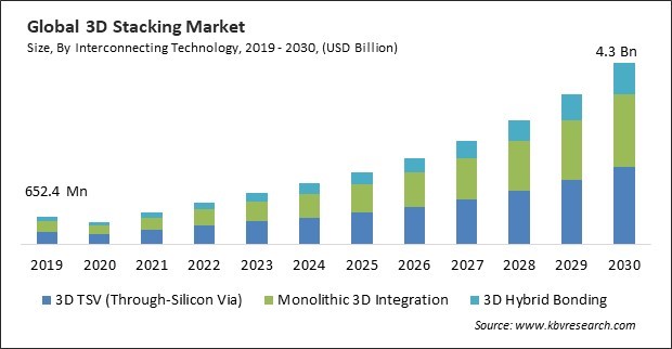
The Global 3D stacking Market size is expected to reach $4.3 billion by 2030, rising at a market growth of 19.8% CAGR during the forecast period.
Wafer-to-wafer bonding allows for stacking entire wafers, which can contain numerous semiconductors dies. This results in significantly higher levels of integration and increased functionality within a single package. Therefore, the Wafer-to-wafer segment captured $132.1 million in 2022. Wafer-level packaging technologies, such as through-silicon vias (TSVs) and fine-pitch bonding techniques, are often employed in W2W stacking. As technology advances, the role of W2W bonding in shaping its future will likely become increasingly significant. Some of the factors impacting the market are heterogeneous integration and component optimization, rapid expansion of semiconductor applications across multiple sectors, and costs and complexity in 3D stacking.

3D stacking enables the integration of different types of semiconductor components, such as processors, memory, sensors, and communication modules, into a single package. This facilitates heterogeneous integration and the creation of multifunctional devices with diverse capabilities. Heterogeneous integration allows for incorporating diverse functionalities within a single package, enhancing the device's overall capabilities. For example, it can combine logic, memory, and sensor functionalities in a compact form factor. This technology offers a range of benefits, including improved performance, energy efficiency, and space savings, making it a versatile solution for various industries. Data centers require high-performance computing solutions to handle increasing data volumes. It provides high memory bandwidth and capacity, improving data processing and energy efficiency. Data analytics, machine learning, and cloud computing benefit from 3D-stacked memory solutions, enabling faster data processing and reducing latency. This, in turn, will drive further growth in the market.
However, 3D stacking involves advanced packaging techniques, which can increase manufacturing costs and complexity. The technology requires investments in specialized equipment and processes. High initial costs are a barrier to entry, especially for smaller companies and startups. Complex manufacturing processes can also lead to production challenges. This involves complex manufacturing processes that differ from traditional 2D semiconductor manufacturing. These processes include wafer thinning, die bonding, TSV formation, and interconnects, each requiring specialized equipment and expertise. The challenges related to costs and complexity are significant factors that impact the market.

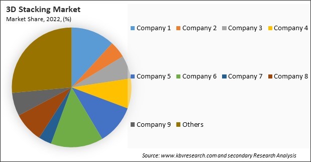
The leading players in the market are competing with diverse innovative offerings to remain competitive in the market. The above illustration shows the percentage of revenue shared by some of the leading companies in the market. The leading players of the market are adopting various strategies in order to cater demand coming from the different industries. The key developmental strategies in the market are Acquisitions, and Partnerships & Collaborations.
Based on interconnecting technology, the market is classified into 3D hybrid bonding, 3D TSV (through-silicon via), and monolithic 3D integration. The 3D hybrid bonding segment acquired a substantial revenue share in the market in 2022. 3D hybrid bonding allows different types of semiconductor die, including logic, memory, sensors, and more, to be stacked together in a single package. This facilitates heterogeneous integration, enabling the creation of complex systems-on-chip (SoCs) with diverse functionalities.
By method, the market is categorized into die-to-die, die-to-wafer, wafer-to-wafer, chip-to-chip, and chip-to-wafer. In 2022, the chip-to-chip segment held the highest revenue share in the market. 3D stacking allows for the integration of various specialized chips into a single package. Chip-to-chip stacking enables the integration of chips from different manufacturers, resulting in heterogeneous chip integration that can offer unique functionalities. By reducing the length of interconnects and enabling closer proximity between chips, it reduces power consumption and heat generation, making it more energy efficient.

On the basis of device type, the market is divided into logic ICs, imaging & optoelectronics, memory devices, MEMS/sensors, LEDs, and others. The LEDs segment garnered a significant revenue share in the market in 2022. LEDs are used for various lighting and display applications. By integrating LEDs into 3D stacked packages, manufacturers create compact, thin devices with built-in lighting or display functionality. This is essential for applications like smartphones, wearables, and automotive displays. LEDs enhance the visual appeal of electronic devices. They are used for backlighting, status indicators, and accent lighting.
By end user, the market is segmented into consumer electronics, manufacturing, communications, automotive, medical devices/healthcare, and others. The automotive segment recorded a remarkable revenue share in the market in 2022. This enables the integration of multiple components and functions within a smaller physical footprint. This can lead to more compact and lightweight electronic control units (ECUs) and sensors in the automotive sector, freeing up space for other vehicle components and reducing overall weight.
| Report Attribute | Details |
|---|---|
| Market size value in 2022 | USD 997.4 Million |
| Market size forecast in 2030 | USD 4.3 Billion |
| Base Year | 2022 |
| Historical Period | 2019 to 2021 |
| Forecast Period | 2023 to 2030 |
| Revenue Growth Rate | CAGR of 19.8% from 2023 to 2030 |
| Number of Pages | 349 |
| Number of Table | 520 |
| Report coverage | Market Trends, Revenue Estimation and Forecast, Segmentation Analysis, Regional and Country Breakdown, Market Share Analysis, Companies Strategic Developments, Company Profiling |
| Segments covered | Type, Technology, Application, Region |
| Country scope | US, Canada, Mexico, Germany, UK, France, Russia, Spain, Italy, China, Japan, India, South Korea, Singapore, Taiwan, Brazil, Argentina, UAE, Saudi Arabia, South Africa, Nigeria |
| Growth Drivers |
|
| Restraints |
|
Region-wise, the market is analyzed across North America, Europe, Asia Pacific, and LAMEA. In 2022, the Asia Pacific region led the market by generating the highest revenue share. Asia Pacific is home to a large and rapidly growing consumer electronics sector. The demand for smaller, more powerful, and energy-efficient devices, such as smartphones, tablets, and wearables, drives the adoption of these technologies to achieve these goals. Asia Pacific, particularly countries like China, Taiwan, South Korea, and Japan, is a global manufacturing hub for semiconductors and electronic components.
Free Valuable Insights: Global 3D Stacking Market size to reach USD 4.3 Billion by 2030
The market research report covers the analysis of key stake holders of the market. Key companies profiled in the report include Taiwan Semiconductor Manufacturing Company Limited, GLOBALFOUNDRIES Inc., Advanced Micro Devices, Inc., Qualcomm, Inc., Intel Corporation, Samsung Electronics Co., Ltd. (Samsung Group), ASE Group (ASE Technology Holding Co., Ltd.), IBM Corporation, Toshiba Corporation, and STMicroelectronics N.V.
By Interconnecting Technology
By Method
By Device Type
By End User
By Geography
This Market size is expected to reach $4.3 billion by 2030.
Heterogeneous integration and component optimization are driving the Market in coming years, however, Costs and complexity in 3D stacking restraints the growth of the Market.
Taiwan Semiconductor Manufacturing Company Limited, GLOBALFOUNDRIES Inc., Advanced Micro Devices, Inc., Qualcomm, Inc., Intel Corporation, Samsung Electronics Co., Ltd. (Samsung Group), ASE Group (ASE Technology Holding Co., Ltd.), IBM Corporation, Toshiba Corporation, and STMicroelectronics N.V.
The expected CAGR of this Market is 19.8% from 2023 to 2030.
The Memory Devices segment is generating highest revenue in the Market by Device Type in 2022; thereby, achieving a market value of $1.3 billion by 2030.
.The Asia Pacific region dominated the Market by Region in 2022, and would continue to be a dominant market till 2030; thereby, achieving a market value of $2.3 billion by 2030.
Our team of dedicated experts can provide you with attractive expansion opportunities for your business.

