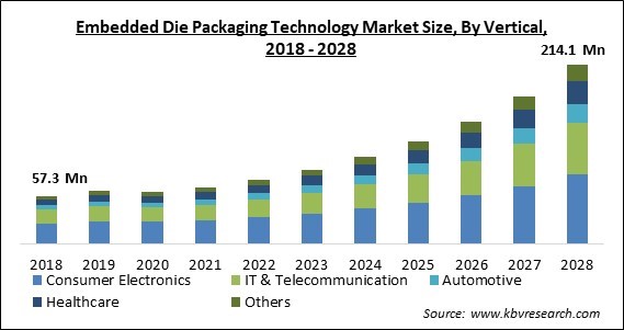
The Global Embedded Die Packaging Technology Market size is expected to reach $214.1 Million by 2028, rising at a market growth of 18.6% CAGR during the forecast period.
System-in-package (SiP) solutions using embedded die packaging technology enable a size reduction of around 70% and are natively 3D-compliant. Miniaturization, enhanced electrical and thermal performance, heterogeneous integration, the potential for cost reduction, and effective OEM logistics are some of this technology's benefits.

Additionally, it provides quick turnaround for customized designs, outstanding robustness, and improved package dependability. Packaging with embedded dies is distinct from other kinds of packaging. Typically, the devices in many IC packages are positioned on top of a substrate. The substrate acts as a link between the devices and aboard in a system. There are several definitions for the phrase "embedded packaging."
However, in embedded die packaging, the concept uses a multi-step manufacturing process to embed components into the substrate. The base of an organic laminate substrate may accommodate the side-by-side integration of a die; many dies, MEMS, or passives. Copper-plated vias are used to link the parts. The board is where the embedded package is located overall, freeing up space in the system.
Embedded die packaging technology uses a multi-step manufacturing process to embed the components into the substrate. In the center of an organic substrate, a die, many dies, or a passive may be placed in a side-by-side configuration. Copper-plated vias, which are located on the board and save up space in the system, are used to link the components. The reduced storage benefit is projected to increase demand for embedded die packaging technology.
The need for embedded die packaging technology results from technological improvements and developments. Embedding technologies meet many criteria, including chip size, electrical performance, and connectivity. In addition, miniaturization allows for more flexible design and more significant board layouts because embedded components may be stacked in several layers with embedded components.
The COVID-19 pandemic outbreak has mixed effects on the Embedded die packaging technology market. Lockdowns have been imposed and extended by the governments of various countries, which has caused production and industrial facilities to shut, creating a crisis and a labor shortage. Therefore, it is determined that the market experienced a decline between 2019 and 2020 after taking into account the opinions of numerous industry experts from different segments of the value chain, including OEMs, suppliers, aggregators, end users, and distributors, in addition to the financial results of different businesses in the embedded die packaging technology ecosystem.
Globally, the downsizing of electrical items is gaining ground quickly. Electronic, portable, lightweight, and lightweight electronic products are becoming more popular with customers. As a result, more people are using fewer electric components. Small form factor electrical components are being used in developing electronic devices to increase available space and enhance the final product design. Customers want portable electronic gadgets that are tiny, modest in size, and packed with functionality. Companies are creating tiny circuits to fit most components onto a single die in order to improve user experience. Customers benefit from enhanced functionality when most components, including sensors and processors, are integrated into a single chip.
Consumer electronics are one of the most widely used goods worldwide. Electronics for non-commercial usage is referred to as consumer electronics. The consumer electronics industry has grown tremendously due to the household sector's increasing adoption of a more extensive range of consumer electronics. Integrating different digital technologies into consumer electronics devices is receiving significant investment from manufacturers, who also place more and more emphasis on giving customers high-quality experiences. In addition, new products with cutting-edge features are being introduced due to the leading market companies' increasing expenditures in R&D and innovation.
The embedded die packaging technique is expensive so it might be a barrier to market expansion. Die packing involves intricate procedures, expensive equipment, and hefty costs. Despite silicon being the second most common material on Earth, wafer packaging is costly. Silicon must be purified before being used to create semiconductor wafers and chips, a complicated procedure that raises costs. Because there are fewer businesses in this industry and fewer rivals due to the growing cost of packaging technologies, this market is vulnerable to abuse.
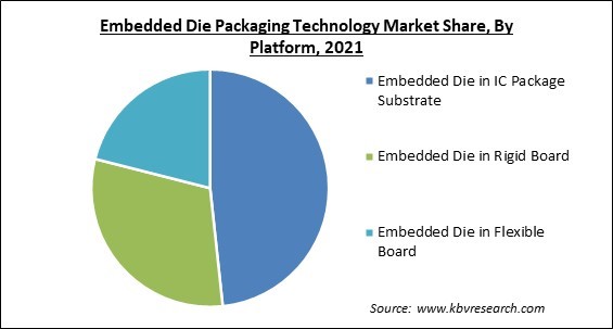
Based on platform, the Embedded Die Packaging Technology Market is divided into Embedded Die in Rigid Board, Embedded Die in Flexible Board, and Embedded Die in IC Package Substrate. The Embedded Die in Flexible Board segment experienced a significant revenue share in 2021. The printed circuit board's product value is rising in line with technological advancements, and sales of flexible boards for use in different wearable and Internet of Things (IoT) devices are anticipated to rise in the future. In addition, flexible circuits are increasingly being embedded for use in several types of small electronic devices.

Based on vertical, the Embedded Die Packaging Technology Market is classified into Consumer Electronics, Automotive, Healthcare, IT & Telecommunications, and Others. The consumer electronics segment contributed the largest revenue share in 2021. Consumer electronics products like home security systems, home appliances, watches, printers, and more are beginning to include embedded systems. Simple embedded systems are used in household appliances like refrigerators, microwaves, and washing machines to give functions, gather user feedback, and regulate items following user preferences.
| Report Attribute | Details |
|---|---|
| Market size value in 2021 | USD 67.2 Million |
| Market size forecast in 2028 | USD 214.1 Million |
| Base Year | 2021 |
| Historical Period | 2018 to 2020 |
| Forecast Period | 2022 to 2028 |
| Revenue Growth Rate | CAGR of 18.6% from 2022 to 2028 |
| Number of Pages | 198 |
| Number of Tables | 280 |
| Report coverage | Market Trends, Revenue Estimation and Forecast, Segmentation Analysis, Regional and Country Breakdown, Companies Strategic Developments, Company Profiling |
| Segments covered | Platform, Vertical, Region |
| Country scope | US, Canada, Mexico, Germany, UK, France, Russia, Spain, Italy, China, Japan, India, South Korea, Singapore, Malaysia, Brazil, Argentina, UAE, Saudi Arabia, South Africa, Nigeria |
| Growth Drivers |
|
| Restraints |
|
Based on region, the Embedded Die Packaging Technology Market is categorized into North America, Europe, Asia Pacific, and LAMEA. The North American region is growing at the promising rate during the forecast period. This is due to the highly developed telecommunications sector, increasing IoT use, and strong development in the automobile sector. In addition, the United States is home to some of the largest automakers in the world that are making investments in the electric vehicle market. With driver assistance features like adaptive cruise control, integrated technologies improve driving comfort.
Free Valuable Insights: Global Embedded Die Packaging Technology Market size to reach USD 214.1 Million by 2028
The market research report covers the analysis of key stake holders of the market. Key companies profiled in the report include General Electric (GE) Co., Infineon Technologies AG, TDK Corporation, Fujikura Ltd., Amkor Technology, Inc., Taiwan Semiconductor Manufacturing Company Limited, ASE Group (ASE Technology Holding), Microsemi Corporation (Microchip Technology), Schweizer Electronic AG (Wus Printed Circuit), and AT&S Group.
By Vertical
By Platform
By Geography
The global Embedded Die Packaging Technology Market size is expected to reach $214.1 Million by 2028.
Increasing demand for smaller electronic devices are driving the market in coming years, however, Associated high costs restraints the growth of the market.
General Electric (GE) Co., Infineon Technologies AG, TDK Corporation, Fujikura Ltd., Amkor Technology, Inc., Taiwan Semiconductor Manufacturing Company Limited, ASE Group (ASE Technology Holding), Microsemi Corporation (Microchip Technology), Schweizer Electronic AG (Wus Printed Circuit), and AT&S Group.
The Embedded Die in IC Package Substrate segment acquired maximum revenue share in the Global Embedded Die Packaging Technology Market by Platform in 2021 thereby, achieving a market value of $100.7 Million by 2028.
The Asia Pacific market dominated the Global Embedded Die Packaging Technology Market by Region in 2021, and would continue to be a dominant market till 2028; thereby, achieving a market value of $92.4 Million by 2028.
Our team of dedicated experts can provide you with attractive expansion opportunities for your business.

