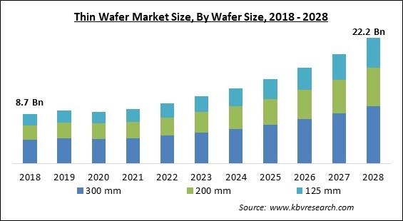
The Global Thin Wafer Market size is expected to reach $22.2 billion by 2028, rising at a market growth of 13.0% CAGR during the forecast period.
While creating integrated circuits, a thin wafer is a slice of semiconductor material. One of the main drivers of a thin wafer market's expansion is the rising demand for semiconductor devices in sectors like telecommunications, consumer electronics, and automotive.

Wafer, also known as a slice or a substrate, is a thin semiconductor slice used in electronics for the production of solar cells and integrated circuits made of crystalline silicon (c-Si). The wafer, which serves as the foundation for those devices, is built inside of and on top. It undergoes numerous microfabrication techniques, such as photolithographic patterning, electrodeposition, doping, etching, and thin-film deposition of various materials. The individual microcircuits are separated by wafer dicing, and they are subsequently assembled into an integrated circuit.
Wafers are made of material that is extremely pure, almost defect-free and has a purity of 99.9999999percentage points (9N) or higher. The C zochralski method, developed by Polish chemist Jan Czochralski, is one method for producing crystalline wafers. Pulling a seed crystal from a melt creates a boule, a cylindrical ingot of a high-purity monocrystalline semiconductor like silicon or germanium. The molten intrinsic material can be doped to create an extrinsic semiconductor of the n-type or p-type by adding donor impurity atoms in exact proportions, such as boron or phosphorus in the case of silicon.
The boule is then cut into wafer-shaped pieces using a wafer saw (a sort of wire saw), machined to increase flatness, chemically erased to remove machining-related crystal damage, and polished to finish. Photovoltaic wafers range in size from 100 to 200 mm square and range in thickness from 100 to 500 m. Electronics employ wafers with diameters ranging from 100 to 450 mm. The largest manufactured wafers are 450 mm in diameter, although they are not yet in widespread use.
The thin wafer industry includes producers of Tier 1 and Tier 2 with manufacturing facilities dispersed across numerous nations. These companies produce thin wafers that are utilized in a variety of end markets, including electronics, automobiles, medical, and a few more. Covid-19 had an impact on both enterprises in the aforementioned sectors as well as thin wafer industry players' operations. The market for MEMS products from the automotive and electronic goods sectors is also anticipated to decrease. The present COVID-19 pandemic has harmed the market for thin wafer processing and dicing equipment, causing a sizable output slowdown as manufacturing activities are momentarily suspended throughout key industrial centers.
Companies all around the world are switching to 5G connectivity to boost operational effectiveness and increase transaction volumes. Additionally, 5G networks can give substantially faster speeds and shorter download times, making them suitable for use in sectors like automotive and smart city development. GaN-based thin wafers, which have the potential to achieve power-added efficiencies (PAE) of 50% or more, are expected to gain popularity. Additionally, it is projected that 5G technology would be widely used in fields like AI, driverless vehicles, and augmented reality. Additionally, the Dutch chipmaker NXP opened a GaN 5G chip manufacturing facility in Arizona intending to enhance 5G communications equipment. This is propelling market expansion.
The introduction of Industry 4.0 and new technologies like IoT and AI in the automobile industry will have a big impact on the expansion of the thin wafer market. The rising need for car connectivity will spur new industry advancements. Additionally, the relevance of linked cars is expanding as a result of current trends like touch-free human-machine interfaces, which are transforming the automotive industry. One of the main drivers of future IoT connection growth is the integration of IoT in vehicle safety and communication technologies. The advent of new technologies including adaptive cruise control, intelligent parking assistance systems, and advanced driver assistance systems (ADAS) will further spur market expansion.
Efficiency is the major problem businesses are currently having while implementing thin wafers. A narrow wafer has poor capability for long-wavelength light absorption, especially if its thickness is less than 50 m. In the case of long wavelengths, the light must travel a great distance before it can be entirely absorbed by the wafer. The main goal in creating a thin wafer was to provide chip makers access to all of its advantages, including high performance, low power consumption, and a smaller die area. Performance is perhaps the biggest challenge that businesses are encountering when deploying thin wafers. The thin wafer has a poor ability for long wavelength absorption, especially if its thickness is less than 50 m. The efficient maintenance of the thin wafers hampers the growth and adoption of the thin wafer market.

Based on the Wafer Size, the Thin Wafer Market is segmented into 125 mm, 200 mm, and 300 mm. The 300 mm segment acquired the highest revenue share in the thin wafer market in 2021. Due to their higher yield, 300 mm wafers are increasingly being used in applications like LED, which is boosting the thin wafer market's expansion. These wafers provide the scale economies and increased profitability that LED makers now find to be necessary. With the help of these wafers, producers may create a large number of products in a single batch.
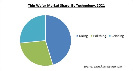
By Technology, the Thin Wafer Market is classified into Grinding, Polishing, and Dicing. The grinding segment recorded a substantial revenue share in the thin wafer market in 2021. To enable stacking and high-density packing of integrated circuits, the wafer thickness is decreased during the semiconductor device manufacture process known as wafer backgrounding (IC). On thin wafers that undergo several processing processes, ICs are created.
Based on the Application, the Thin Wafer Market is bifurcated into MEMS, CIS, Memory, RF Devices, LED, Interposer, Logic, and Others. The memory segment garnered the highest revenue share in the thin wafer market in 2021. Memory has relied mainly on a mixture of blades and laser dicing to separate complicated stacks. The high metal concentration causes delamination problems when just blade dicing is used on top layers. However, it is challenging to simulate 50 m thin wafers safely.
| Report Attribute | Details |
|---|---|
| Market size value in 2021 | USD 9.6 Billion |
| Market size forecast in 2028 | USD 22.2 Billion |
| Base Year | 2021 |
| Historical Period | 2018 to 2020 |
| Forecast Period | 2022 to 2028 |
| Revenue Growth Rate | CAGR of 13% from 2022 to 2028 |
| Number of Pages | 228 |
| Number of Tables | 400 |
| Report coverage | Market Trends, Revenue Estimation and Forecast, Segmentation Analysis, Regional and Country Breakdown, Companies Strategic Developments, Company Profiling |
| Segments covered | Wafer Size, Technology, Application, Region |
| Country scope | US, Canada, Mexico, Germany, UK, France, Russia, Spain, Italy, China, Japan, India, South Korea, Singapore, Malaysia, Brazil, Argentina, UAE, Saudi Arabia, South Africa, Nigeria |
| Growth Drivers |
|
| Restraints |
|
Region-wise, the Thin Wafer Market is analyzed across North America, Europe, Asia Pacific, and LAMEA.The Asia Pacific segment acquired the highest revenue share in the thin wafer market in 2021. Due to China's and Japan's explosive growth in the use of high-end consumer goods, including smartwatches and smart home gadgets. Due to good economic conditions and rising consumer electronics demand, the Asia Pacific region is predicted to experience significant growth in the semiconductor market.
Free Valuable Insights: Global Thin Wafer Market size to reach USD 22.2 Billion by 2028
The market research report covers the analysis of key stake holders of the market. Key companies profiled in the report include Shin-Etsu Chemical Co., Ltd., SUMCO Corporation, GlobalWafers Co., Ltd., Siltronic AG, SK Siltron Co., Ltd., SUSS MicroTec SE, Soitec, DISCO Corporation, 3M Company, and Applied Materials, Inc.
By Wafer Size
By Technology
By Application
By Geography
The global Thin Wafer Market size is expected to reach $22.2 billion by 2028.
Smaller Electrical Device Sizes High 5g Technology Adoption are driving the market in coming years, however, The Maintenance Of Narrow Wafer Efficiency Is A Critical Issue restraints the growth of the market.
Shin-Etsu Chemical Co., Ltd., SUMCO Corporation, GlobalWafers Co., Ltd., Siltronic AG, SK Siltron Co., Ltd., SUSS MicroTec SE, Soitec, DISCO Corporation, 3M Company, and Applied Materials, Inc.
The Dicing market acquired the high revenue share in the Global Thin Wafer Market by Technology in 2021, thereby, achieving a market value of $9.8 billion by 2028.
The MEMS market shows the high growth rate of 13.4% during (2022 - 2028).
The Asia Pacific market dominated the Global Thin Wafer Market by Region in 2021, and would continue to be a dominant market till 2028; thereby, achieving a market value of $8.2 billion by 2028.
Our team of dedicated experts can provide you with attractive expansion opportunities for your business.

