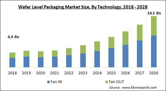
The Global Wafer Level Packaging Market size is expected to reach $14.1 billion by 2028, rising at a market growth of 17.7% CAGR during the forecast period.
Wafer level packaging (WLP) is a technique for connecting packaging elements to an integrated circuit before slicing it. Unlike the traditional approach, which involves slicing the wafer into individual circuits before attaching the packaging components, this procedure does not include slicing the wafer into distinct circuits. Factors such as increased usage of high-speed, compact-size, and less expensive electronic goods are expected to propel the worldwide wafer level packaging business forward. Furthermore, the technological superiority of wafer level packaging over traditional packaging approaches, as well as the approaching requirement for circuit downsizing in microelectronic devices, drive market growth. Moreover, the increased utilization of wafers throughout the automotive industry is anticipated to drive the market.
Wafer-level packaging entails extending wafer fabrication methods to include device connectivity and protection. Most alternative types of packaging start with wafer dicing and then place the individual die in a plastic box with solder bumps attached. Wafer-level packaging entails attaching the bottom and top outer layers of packaging, as well as the solder bumps, onto integrated circuits while the wafer is still in the wafer, and then slicing the wafer. At the moment, there is no one industry-standard approach to wafer-level packaging. Because of their small size, cellphones are a popular application for WLPs.
Because of the rapid advancements in integrated circuit manufacturing processes, fans in wafer level packaging solutions are becoming increasingly significant in the semiconductor packaging area. Moreover, one of the primary drivers driving the market for wafer level packaging solutions is the demand for faster, lighter, smaller, and more cost-effective electronic equipment with high performance as well as low-cost packaging. WLP can be found in consumer electronic devices such as cellphones and other semiconductor devices, as well as in ICs. One of the primary elements driving demand for wafer level packaging technology over traditional packaging solutions is the growing demand for technical improvement in mobile devices that are capable of completing a variety of programs in a single small-end product.

The COVID-19 outbreak had a considerable impact on the semiconductor and electronics industries. Due to an increase in the number of COVID-19 cases, business and manufacturing facilities in several nations were closed during the pandemic. Additionally, the partial and complete travel restrictions impacted the worldwide supply chain, making it difficult for manufacturers to access customers. The COVID-19 outbreak had a global impact on society and the economy. The impact of this pandemic was growing rapidly, and it affected worldwide business. The crisis has wreaked havoc on the stock market, causing a drop in corporate confidence, a major slowdown in the supply chain, and an increase in customer concern. Due to the shutdown of production operations, various countries under the lockdown lost a significant amount of business and money.
Electrical testing is less expensive and takes less time because these programs were designed with DFT in mind. Because the connections are exposed on the wafer, advanced fabs can automate this procedure, and testing is not required after packaging. Burn-in testing is also accelerated due to the utilization of a single wafer. The IC verification method includes two critical steps, including assessing reliability and functional testing. Wafer-level packaging was not designed specifically to improve DFT, but it undoubtedly helps because it exposes critical test locations and interconnects directly on the wafer.
When the casting solutions are efficiently emerging from the film, imidization rates can be better regulated. Controlled and regulated temperature ramp rates provide an enhanced system window for optimal polyimide film curing. When using many layers of polyimide, optimal temperature control is very important. Due to tension, improper curing can cause the first polyimide layer to soften and the metal lines to wrinkle. Absorption of oxygen in the polyimide can result in a dark, brittle coating. Vacuum / N2 cycles generate an oxygen-free environment for curing. The diameter of the intermediate wafer determines the investment and manufacturing infrastructure in traditional WLCSP processing.
Various wafer level packaging, or WLP, technologies are currently being introduced in the market at an extremely high altitude, particularly in portable and mobile applications. In recent years, a considerable number of wafer level packaging units were installed in smartphones, tablet PCs, and portable gadgets, indicating a significant rise in the wafer level packaging industry. However, there are several challenges that are being posed to the market players operating in this sector. one of the major challenges is that wafer level packaging requires a higher capital investment than traditional flip-chip and wire bonding packaging since it uses fab-like tools for the redistribution process using thin layer metals and dielectric polymers. Cost reduction is a significant aspect of expanding the market beyond its present limitations.

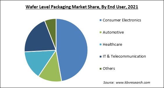
Based on End User, the market is segmented into Consumer Electronics, Automotive, Healthcare, IT & Telecommunication, and Others. In 2021, the consumer electronics segment recorded the largest revenue share of the wafer level packaging market. The constantly increasing growth of this segment is attributed to the advancements in electronic packaging technology, which have resulted in highly efficient and robust electrical interconnect methods for electronic products.
Based on Type, the market is segmented into WLCSP, 2.5D TSV WLP, 3D TSV WLP, Nano WLP, and Others. In 2021, the 2.5D TSV WLP segment garnered a substantial revenue share of the wafer level packaging market. The increased capacity, reduced system space requirements, improved performance, and low power consumption are all characteristics that contribute to the widespread use of 2.5D TSV WLP. This factor would aid in increasing the growth of this segment across the market in the forecast years.
Based on Technology, the market is segmented into Fan IN and Fan OUT. In 2021, the Fan-in WLP segment witnessed the largest revenue share of the wafer level packaging market. The increasing growth of this segment is attributed to the st4rong position of Fan-in WLP technology in the semiconductor sector, offering undeniable benefits in terms of shape and cost. Moreover, technological improvement and innovation continue to expand the range of fan-in WLP solutions. The growing use and use of fans in wafer level packaging across automotive, consumer electronics, and industrial applications are driving the demand for sophisticated fan-in WLP solutions around the world. Furthermore, the IoT (Internet of Things) promises a plethora of new applications for which fan-in WLP would be an ideal option, presenting a lucrative chance to further boost the demand.
| Report Attribute | Details |
|---|---|
| Market size value in 2021 | USD 4.7 Billion |
| Market size forecast in 2028 | USD 14.1 Billion |
| Base Year | 2021 |
| Historical Period | 2018 to 2020 |
| Forecast Period | 2022 to 2028 |
| Revenue Growth Rate | CAGR of 17.7% from 2022 to 2028 |
| Number of Pages | 213 |
| Number of Tables | 380 |
| Report coverage | Market Trends, Revenue Estimation and Forecast, Segmentation Analysis, Regional and Country Breakdown, Companies Strategic Developments, Company Profiling |
| Segments covered | Type, Technology, End User, Region |
| Country scope | US, Canada, Mexico, Germany, UK, France, Russia, Spain, Italy, China, Japan, India, South Korea, Singapore, Malaysia, Brazil, Argentina, UAE, Saudi Arabia, South Africa, Nigeria |
| Growth Drivers |
|
| Restraints |
|
Based on Regions, the market is segmented into North America, Europe, Asia Pacific, and Latin America, Middle East & Africa. In 2021, Asia-Pacific accounted for the largest revenue share of the wafer level packaging market. The growth of the regional market is majorly attributed to the fact that Taiwan is home to some of the world's largest semiconductor manufacturers, fueling demand for sophisticated semiconductor packaging, particularly in PLPs. According to the Semiconductor Industry Association (SIA), this region accounts for more than half of worldwide semiconductor sales, giving Taiwanese manufacturers more opportunities to supply FOWLP for growing semiconductor applications. The majority of enterprises in the country are expanding their Fan-out packaging production capacity, which is projected to boost exports while also helping to strengthen the local market.
Free Valuable Insights: Global Wafer Level Packaging Market size to reach USD 14.1 Billion by 2028
The market research report covers the analysis of key stake holders of the market. Key companies profiled in the report include ASML Holding N.V., Fujitsu Limited, Toshiba Corporation, Qualcomm, Inc., Amkor Technology, Inc., Deca Technologies, Inc., Jiangsu Changjing Electronics Technology Co., Ltd., Tokyo Electron Ltd., Applied Materials, Inc., and Lam Research Corporation.
By End User
By Type
By Technology
By Geography
The global wafer level packaging market size is expected to reach $14.1 billion by 2028.
Optimizes temperature control are increasing are driving the market in coming years, however, requirement for high initial investment growth of the market.
ASML Holding N.V., Fujitsu Limited, Toshiba Corporation, Qualcomm, Inc., Amkor Technology, Inc., Deca Technologies, Inc., Jiangsu Changjing Electronics Technology Co., Ltd., Tokyo Electron Ltd., Applied Materials, Inc., and Lam Research Corporation.
The expected CAGR of the wafer level packaging market is 17.7% from 2022 to 2028.
The WLCSP segment acquired maximum revenue share in the Global Wafer Level Packaging Market by Type in 2021, thereby, achieving a market value of $5.3 billion by 2028.
The Asia Pacific is the fastest growing region in the Global Wafer Level Packaging Market by Region in 2021.
Our team of dedicated experts can provide you with attractive expansion opportunities for your business.

